- 您现在的位置:买卖IC网 > Sheet目录1994 > DS2187S+ (Maxim Integrated Products)IC RECEIVE LINE INTERFACE 20SOIC
DS2187
3 of 10
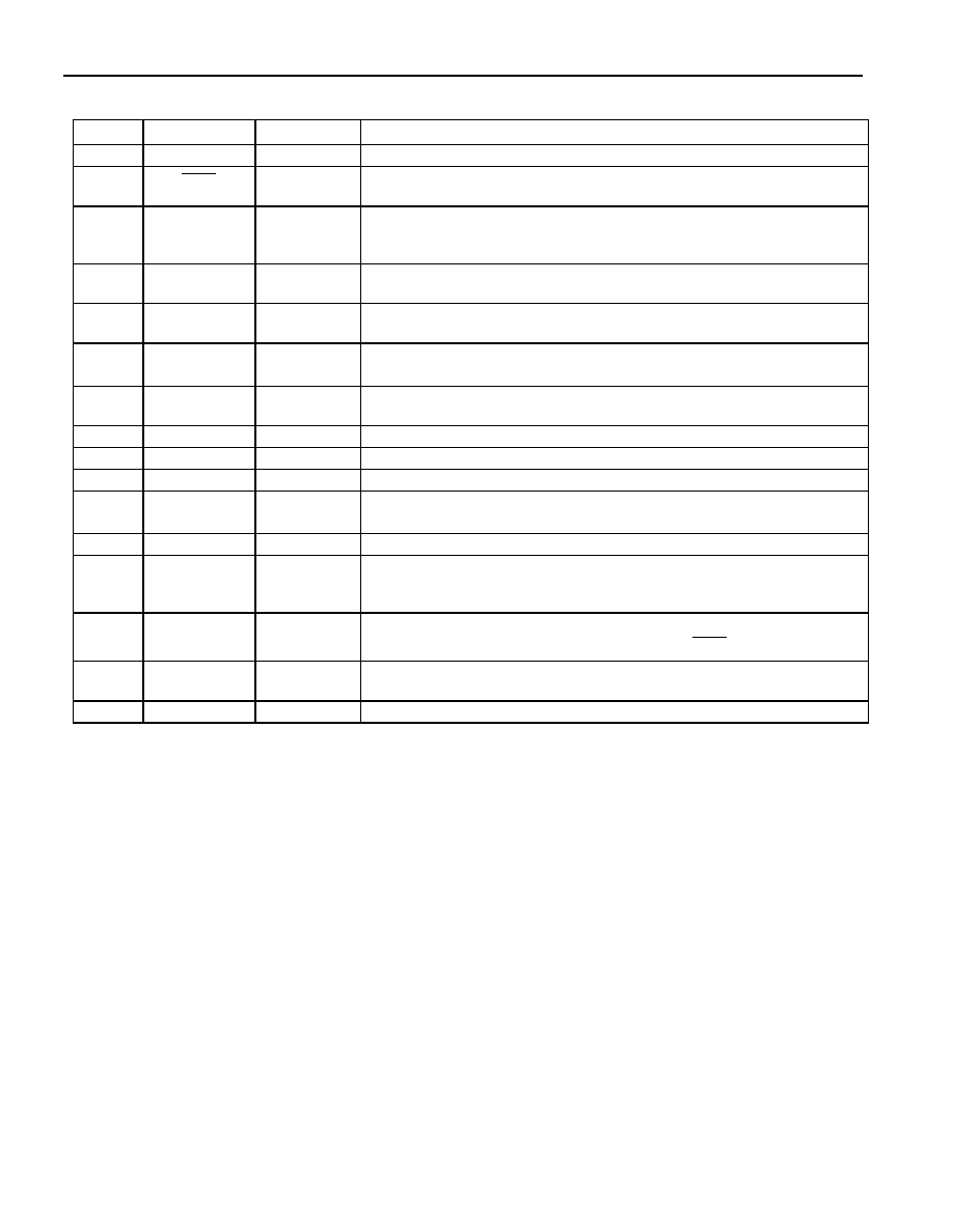
PIN DESCRIPTION Table 1
PIN
SYMBOL
TYPE
DESCRIPTION
1AVDD
-
Analog Positive Supply. 5.0 volts.
2
RAIS
I
Reset Alarm Indication Signal.
Every other low pulse at this input
establishes the AIS alarm detection period.
3
ZCSEN
I
0 Code Suppression Enable.
When high, incoming B8ZS (RCLKSEL=0)
or HDB3 (RCLKSEL=1) code words are replaced with all 0s at RPOS and
RNEG; when low, no code replacement occurs.
4LCAP
-
Loop Cap.
Part of internal loop filter; attach a 10 microfarad capacitor from
this pin to VSS.
5
RCLKSEL
I
Receive Clock Select.
Tie to VSS for 1.544 MHz (T1) applications, to VDD for
2.048 MHz (CEPT) applications.
6
7
RTIP
RRING
I
Receive Tip and Ring.
Connect to line transformer as shown in Figure 2.
8
LOCK
O
Frequency Lock.
High state indicates that internal circuitry is phase- and
frequency-locked to the incoming signal at RRING and RTIP.
9
AVSS
-
Analog Signal Ground.
0.0 volts.
10
DVSS
-
Digital Signal Ground.
0.0 volts.
11
RCLK
O
Receive Clock.
Extracted line rate clock.
12
13
RNEG
RPOS
O
Receive Data.
Extracted receive data; updated on rising edge of RCLK.
14
NC
-
No Connect.
Do not connect to this pin.
15
BPV
O
Bipolar Violation.
Transitions high for the full bit period when a bit in
violation appears at RPOS or RNEG; B8ZS code words are not accused when
ZCSEN=1. BPV not valid for RCLKSEL=1 and ZCSEN=1.
16
AIS
O
Alarm Indication Signal.
High when the received data stream has contained
less than three 0s during the last two periods of the RAIS signal.
17
RCL
O
Receive Carrier Loss.
High if 192 0s appear at RPOS and RNEG; reset on
next occurrence of a one.
18
DVDD
-
Digital Positive Supply.
5.0 volts
发布紧急采购,3分钟左右您将得到回复。
相关PDF资料
DS21Q58L
IC TXRX E1 QUAD 3.3V 100-LQFP
DS2404B
IC ECONORAM TIMECHIP 5.5V 16SSOP
DS2415P+T&R
IC TIME CHIP 1-WIRE 6-TSOC
DS2417X/T&R
IC TIMECHIP W/INTRPT 1WIRE CSP
DS26502LN+
IC T1/E1/J1 64KCC ELEMENT 64LQFP
DS26503LN+
IC T1/E1/J1 BITS ELEMENT 64-LQFP
DS3105LN+
IC TIMING LINE CARD 64-LQFP
DS3106LN+
IC TIMING LINE CARD 64-LQFP
相关代理商/技术参数
DS2188
功能描述:通信集成电路 - 若干 RoHS:否 制造商:Maxim Integrated 类型:Transport Devices 封装 / 箱体:TECSBGA-256 数据速率:100 Mbps 电源电压-最大:1.89 V, 3.465 V 电源电压-最小:1.71 V, 3.135 V 电源电流:50 mA, 225 mA 最大工作温度:+ 85 C 最小工作温度:- 40 C 封装:Tube
DS2188+
功能描述:通信集成电路 - 若干 RoHS:否 制造商:Maxim Integrated 类型:Transport Devices 封装 / 箱体:TECSBGA-256 数据速率:100 Mbps 电源电压-最大:1.89 V, 3.465 V 电源电压-最小:1.71 V, 3.135 V 电源电流:50 mA, 225 mA 最大工作温度:+ 85 C 最小工作温度:- 40 C 封装:Tube
DS2188N
功能描述:通信集成电路 - 若干 RoHS:否 制造商:Maxim Integrated 类型:Transport Devices 封装 / 箱体:TECSBGA-256 数据速率:100 Mbps 电源电压-最大:1.89 V, 3.465 V 电源电压-最小:1.71 V, 3.135 V 电源电流:50 mA, 225 mA 最大工作温度:+ 85 C 最小工作温度:- 40 C 封装:Tube
DS2188S
功能描述:通信集成电路 - 若干 RoHS:否 制造商:Maxim Integrated 类型:Transport Devices 封装 / 箱体:TECSBGA-256 数据速率:100 Mbps 电源电压-最大:1.89 V, 3.465 V 电源电压-最小:1.71 V, 3.135 V 电源电流:50 mA, 225 mA 最大工作温度:+ 85 C 最小工作温度:- 40 C 封装:Tube
DS2188S/T&R
功能描述:通信集成电路 - 若干 RoHS:否 制造商:Maxim Integrated 类型:Transport Devices 封装 / 箱体:TECSBGA-256 数据速率:100 Mbps 电源电压-最大:1.89 V, 3.465 V 电源电压-最小:1.71 V, 3.135 V 电源电流:50 mA, 225 mA 最大工作温度:+ 85 C 最小工作温度:- 40 C 封装:Tube
DS2188S+
功能描述:通信集成电路 - 若干 RoHS:否 制造商:Maxim Integrated 类型:Transport Devices 封装 / 箱体:TECSBGA-256 数据速率:100 Mbps 电源电压-最大:1.89 V, 3.465 V 电源电压-最小:1.71 V, 3.135 V 电源电流:50 mA, 225 mA 最大工作温度:+ 85 C 最小工作温度:- 40 C 封装:Tube
DS2188S+T&R
制造商:Maxim Integrated Products 功能描述:T1/CEPT JITTER ATTENUATOR 16SOIC W - Tape and Reel
DS2188S+T&R
功能描述:通信集成电路 - 若干 RoHS:否 制造商:Maxim Integrated 类型:Transport Devices 封装 / 箱体:TECSBGA-256 数据速率:100 Mbps 电源电压-最大:1.89 V, 3.465 V 电源电压-最小:1.71 V, 3.135 V 电源电流:50 mA, 225 mA 最大工作温度:+ 85 C 最小工作温度:- 40 C 封装:Tube